This article is based on the references and idea from Dr. Zhen Zhou and Prof. Yang Yi, thank you for your guidance and help.
- Wave physics as an analog recurrent neural network1
- A Radio Frequency Analog Computer for Computational Electromagnetics2
- Universal Chiplet Interconnect Express (UCIe): An Open Industry Standard for Innovations With Chiplets at Package Level3
- Challenges and recent prospectives of 3D heterogeneous integration4
- Chiplet Technology and Heterogenous Integration5
- Chiplet Technology & Heterogeneous Integration6
Overview
UCIe is short for Universial Chiplet Interconnect Express7. UCIe Cononsortium provides whitepapers for V1.08 as well as for V1.19. Intel’s Dr. Debendra Das Sharma10 writes the paper that defines UCIe. In addition, it provides webinars11 by embedding YouTube videos in the webpage. UCIe Consortium also has a YouTube channel12 that contains lots of useful tutorials. Spepcifications13 could not be accessed to the general public as only employees of partners are able to see.
The following table provides a high level overview of UCIe architecture from both hardware perspective on the left side to the software protocol stack on the right side of the table.
| PHY | RDI | D2D Adapter | FDI | Protocol | |
| name | Physical Layer | Raw Die to Die Interface | Die to Die Adapter | Flit-aware Die to Die Interface | Protocol Layer |
| Concepts8 | 1️⃣Link Traning 2️⃣Lane Repair 3️⃣Lane Reversal 4️⃣Scrambling 5️⃣Sidband 6️⃣Analog Front End 7️⃣Clock Forwarding | 1️⃣ARB/MUX 2️⃣CRC/Retry 3️⃣Link State Mgmt 4️⃣Parameter Negotiation | 1️⃣PCIe14 2️⃣CXL1516 🔹CXL.io 🔹CXL.cache 🔹CXL.mem 3️⃣Streaming17 4️⃣Raw | ||
| Extension | Packaging | Flit |
| PHY | D2D | Protocol | |
| CXL | ARB/MUX | ||
| CRC | lightweight 16 bit triple bit detection, converge at high frequency, pipeline. | ||
| RETRY | simplify from | ||
| LSM20 | Link state management: Reset/Active/PowerMgmt/Error flows | ||
| PN21 | PN with remote link partner22 | ||
| PCI | |||
| CXL | |||
| Steaming | support Raw formats |
Hardware
This section discusses the hardware aspect of UCIe™ as well as advanced packaging for chiplets.
Packaging
Packaging for integrated circuit contains knowledge and technology from various aspects, the following table is aiming to summarize the different categories of technology on chiplets packaging.
| Categories | Details | |||
| Die/Package Stacking | 2.5D, 3D Die Thinning/Stacking Package on Package Package in Package | |||
| Wafer Level Package | Wafer Bumping Cu Pillar Fan-out WLP Wafer Level IPD Wafer Level MEMS | |||
| Interconnection | Cap Wire Bond Wire Bond Flip Chip | |||
| Embedded Substrate | SESUB a-EASI | |||
| Double Side Molding | Double Side Molding Selective Molding Flexible Encapsulation Molded Underfill Irregular Packaging | |||
| Antenna | Antenna on Package Antenna in Package | |||
| Board Assembly | High Density SMT ACF Bonding Wire Bond on Flex Laser Welding Flex Bending | |||
| Shielding | Conformal Shielding Compartment Shielding Selective Shielding Magnetic shielding |
UCIe V1.08 supports 2 types of packaging, namely standard package(UCIe-S) and advanced package(UCIe-A).
| Standard Package | Advanced Package | |
| Characteristics | ||
| Data Rate per Lane(GT/s)24 | 4, 8, 12, 16, 24, 32 | 4, 8, 12, 16, 24, 32 |
| Width/Configuration(each cluster) | 16 Full Duplex | 64 Full Duplex |
| Bump pitch(\(\mu m\)) | 100-130 | 25-55 |
| Channel Reach(\(mm\)) | \(10\leqslant L \leqslant 25\) | \(\leqslant 2\) |
| Raw Bit Error Rate(BER) | ◾️\(10^{27}\) 16GT/s short reach ◾️\(10^{15}\) 16GT/s long reach | ◾️\(10^{27}\) 12GT/s ◾️\(10^{15}\) 16GT/s |
| Targets for Key Metrics | ||
| B/W Shoreline(\(GB/s/mm\)) | 28-224 | 165-1317 |
| B/W Density(\(GB/s/mm^{2}\)) | 22-125 | 188-1350 |
| Bump | ||
| bump maps!! | ◾️\(\times16\) ◾️\(\times32\) | ◾️8-columns, ◾️10-columns ◾️16-columns ❗️UCIe-A area/column type efficiency plots25 |
UCIe™ at the moment(V1.1) only supports 2D and 2.5D packaging, 2 figures are placed in this article for illustration purpose. The following figure Figure 4: UCIe : Layering Approach and different packaging choices is extracted from V1.0 of whitepaper8.
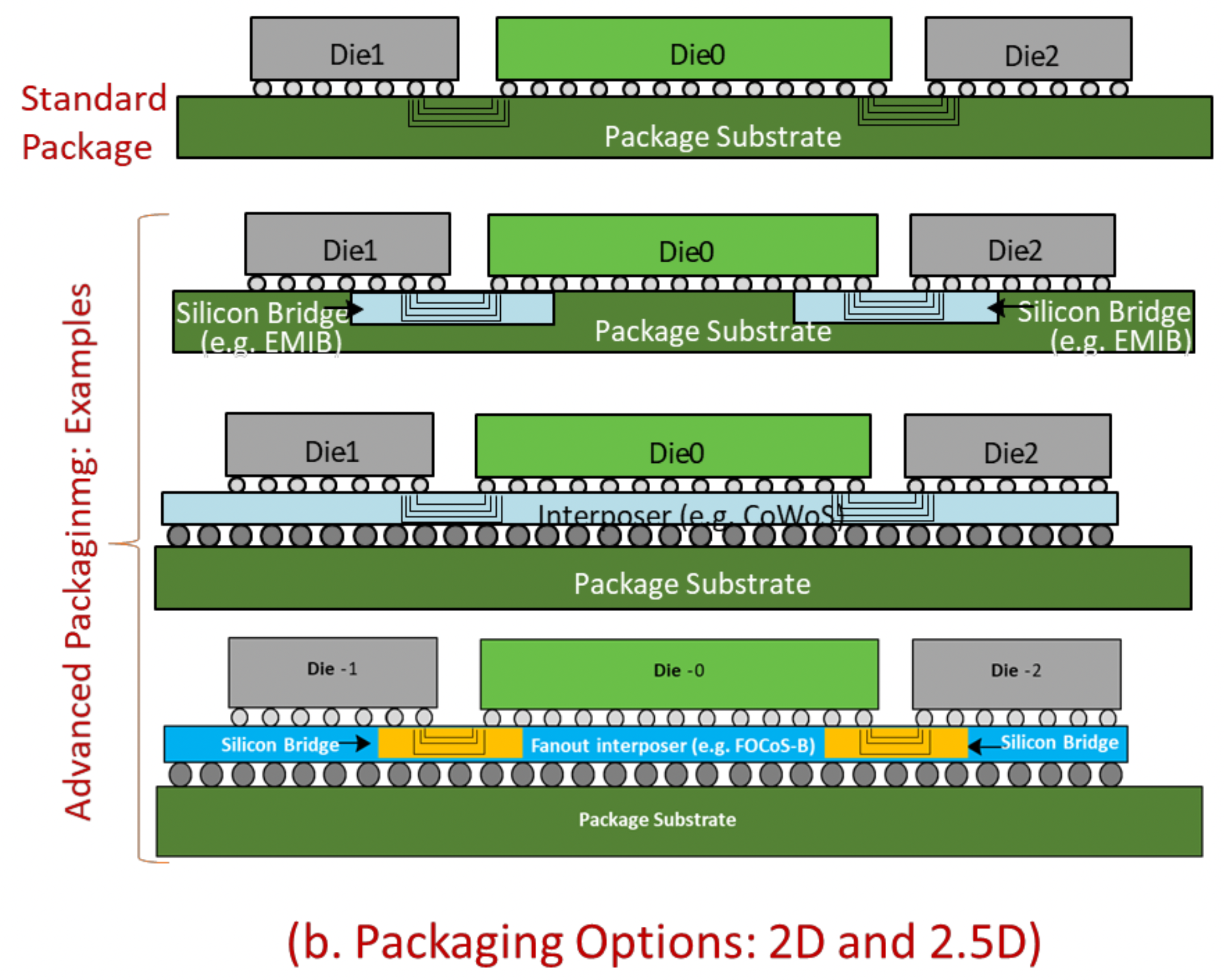
The standard/laminate packaging (2D) is used for cost-effective performance. The advanced packaging(2.5D) is used for power-efficient performance. There are multiple commercially available options, some of which are shown in the diagram. UCIe specification embraces all types of packaging choices in these categories.
Universal Chiplet Interconnect Express (UCIe)®: Building an open chiplet ecosystem8
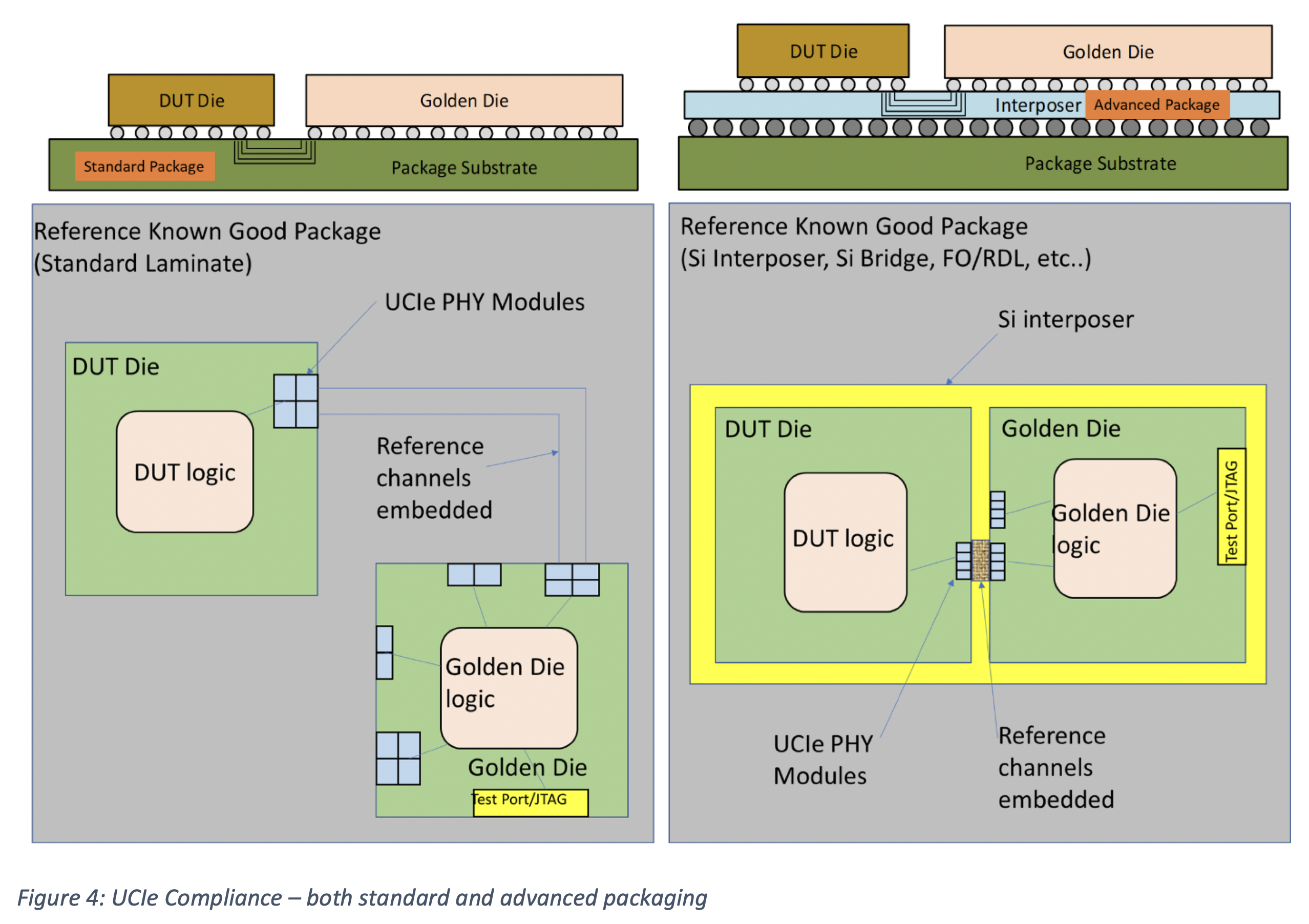
The following figure is from Figure 4 of V1.1 whitepaper9.
Heterogeneous Integrations
There are several books that give a comprehensive description on heterogeneous integration which enable readers to quickly learn about the basics of problem-solving methods and understand the trade-offs inherent in making system-level decisions.
“Heterogeneous Integrations”28
“Chiplet Design and Heterogeneous Integration Packaging”29
_https://semiengineering.com/is-ucie-really-universal/
https://www.computer.org/csdl/magazine/mi/2023/02/10013705/1JP1z96RPP2
_https://docs.pingcode.com/info/34526.html
UCIe-S Bump map
The video30 explains the routing of UCIe-S bump maps with details.
checkboard arrangement is useful for interrupt concerns, mechanical compatibility.
UCIe-A area/column type efficiency plots31
UCIe-A interoperability across bump pitch range32: fixed beachfront, signal ordering rules.
UCIe considers not only the protocol software side, the hardware side regarding electrical and packaging are highly emphasized for chiplets design.
Flit mean flow control unit.
CXL: compute express link33
Wafer Level Packaging
Fan-In
Fan-Out: any package with connections fanned-out of the chip surface, enabling more external I/Os.34 A comparision of Fan-In and Fan-Out illustration for a RF module.35
FOWLP: Fan-Out Wafer Level Packaging, this image36 shows how the FOWLP based chip is made.
Interposer37
Interposer contains the following characteristics:
- Purpose: electronic substrate to interconnect between the fine-pitch I/Os at the die level on the top side to the coarser dimensional features on the package on the bottom side of the interposer.37
- TSV: Through-silicon Via, illustration of TSV on High Bandwidth Mememory38, in reference39 page 10 figure 17, illustrations of how RDL is manufactured is presented.
- TPV: Through-package Via
- RDL: redistribution layers on both sides of the interposer, in reference39 page 10 figure 16, illustrations of how RDL is manufactured is presented.
Through-silicon Via40
- Via First
- Via Middle
- Via Last
Advanced Packaging Technology
There is an incredible number of advanced packaging types and brand names from Intel (EMIB, Foveros, Foveros Omni, Foveros Direct), TSMC (InFO-OS, InFO-LSI, InFO-SOW, InFO-SoIS, CoWoS-S, CoWoS-R, CoWoS-L, SoIC), Samsung (FOSiP, X-Cube, I-Cube, HBM, DDR/LPDDR DRAM, CIS), ASE (FoCoS, FOEB), Sony (CIS), Micron (HBM), SKHynix (HBM), and YMTC (XStacking).
Advanced Packaging Part 2 – Review Of Options/Use From Intel, TSMC, Samsung, AMD, ASE, Sony, Micron, SKHynix, YMTC, Tesla, and Nvidia41
| Technology | Corporation | Category | |
| EMIB4243 | Intel | 2.5D | 🔵thin pieces of silicon with multi-layer BEOL44 interconnects, embedded in organic substrates. Fig 4(A)43 ❗️limitations of interposer SI and enable similar inter-die bandwidth at lower cost45 |
| Foveros4647 | Intel | 2.5D/3D48 | 🔬49, with EMIB named Co-EMIB50 🔵F2F \(\mu\)bumps for Foveros 🔵Cu Column for Foveros Omni |
| Foveros Direct | Intel | Hybrid Bonding48 | 🔵Cu to Cu Bonding for Foveros Direct51 |
| ODI5245 | Intel | 3D | 🔵Type I: sharing 🔵Type II: single die 🔵Cupper Pillar or Package |
| CoWoS53 | TSMC | 2.5D Package Chip Last | 🔬54, CoWoS®-S structure55, NEC SX-Aurora56, high-K MiM57, iCAP58 AMD EPYC MI30059🔬60 |
| CoWoS-R61 | TSMC | 2.5D Package Chip Last | 🔬62, 🔴InFO technology to utilize RDL interposer which comprised of polymer and copper traces. 🔴Build bigger chips: adding high-bandwidth memory (HBM) stacks to one or more processors.63 |
| CoWoS-L64 | TSMC | 2.5D Package Chip Last | 🔬65, 🔴interposer with LSI66 chip 🔴RDL layers for power and signal delivery |
| InFO67 | TSMC | Package Chip First | 🔴InFO_oS68: LSI66+RDL 🔴InFO_PoP🔬69: FOWLP70+PoP71, DRAM TIV72 connect to Fan-Out processor. InFO_B73 ❗️InFO_PoP vs CoWoS vs SoIC🔬74 🔴InFO_LSI: InFO_oS+LSI on Substrate66 🔴InFO_SoIS: System-on-Integrate Substrate55 🔴InFO_SoW: System-on-Wafer |
| SoIC75 | TSMC | 3D Chip Stack76 | 🔴CoW77: 🔴WoW78: bond face to face with same size79. ❗️CoW and WoW comparison: 🔬80 ❗️SoIC: Fronend, chiplet; InFO&CoWoS: Backend, integration. AMD EPYC MI30059🔬60 |
| I-Cube81 | Samsung82 | 2.5D | |
| H-Cube83 | Samsung | 2.5D | |
| X-Cube84 | Samsung | 3D | ⚪️compete with SoIC |
| ASE | |||
| Sony | |||
| Micron | |||
| SKHynix85 | |||
| YMTC86 |
Concepts for packaging
2.5D vs 3D: The major difference between 2.5D and 3D are 2.5D uses passive silicon where 3D uses active silicon which not only has electrical connections but has integrated circuits as well.87 In 2.5D structure, two or more active semiconductor chips are placed side-by-side on a silicon interposer for achieving extremely high die-to-die interconnect density. In 3D structure, active chips are integrated by die stacking for shortest interconnect and smallest package footprint.88 2.5D strcture needs interposer while 3D strcture enables direct vertical connection between dies at page 11 of 39.
chip first vs chip last: InFO is a chip first process where the chip is placed first, then build the RDLs are built around it. With CoWoS, the RDLs are built up then the chip is placed.
Hybrid Packaging
Optics and UCIe: the article89 figure 6 contains the evolution of integration between optical data connection and IC to have larger bandwitdh for Co-packaged datacenter optics.
| Raw | Standard 256 bit flit mode | ||
| Stream | ✅ only90 | ||
PHY Layer
Module
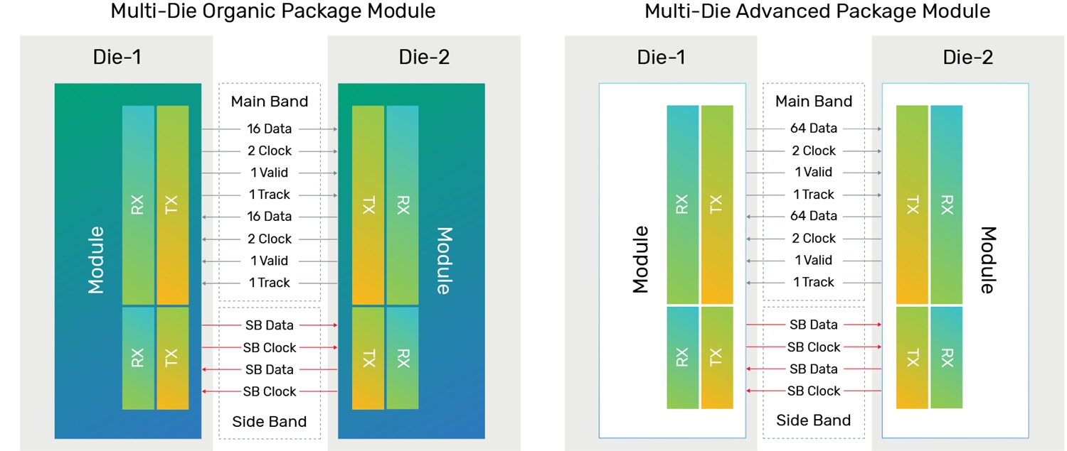
A pair of physical interface between dies is defined as module, with main band for data transfer and side band for connection overhead.
The following figure91 shows the connection of modules for UCIe-S as well as UCIe-A.
- UCIe-S: 16TX, 16 RX, Side Band DATA, CLK
Die 2 Die Adapter
Flit formats
Contents
flit header carries: protocol identifier, stack identifier92, sequence number, Ack/Nak completion, pause of data stream indication.
pause of data stream indication(PDS): as for 68 byte size is note a multiple of lane numbers, an pause indication is needed, which is a dedicated header followed by all 0 for receiver to react.
Types
Raw format: bypass D2D which can be used directly on PHY layer.
68 Flit format: this stems form CXL flit format, 64 bytes from FDI, 4 bytes inserted in D2D, 2 bytes of flit header, 2 bytes of CRC, data shifting to for RDI as it allows 64 bytes flit size.
Standard 256B End Header Flit Format: this design is related to how data buffer works thus header is placed at the end.
Standard 256B Start Header Flit Format: CXL 256 Flit Model protocol
Latency Optimized 256B without Optional bytes:
Latency Optimized 256B with Optional bytes:
| Format | Name | PCIe Non-Flit Mode | PCIe Flit Mode | CXL 68B Flit Mode | CXL 256B Flit Mode | Streaming17 |
| 1 | Raw | Optional | Optional | Optional | Optional | Mandatory |
| 2 | 68B | Mandatory | 🚫 | Mandatory | 🚫 | 🚫8, ✅9 |
| 3 | Std 256B End Header | 🚫 | Mandatory | 🚫 | 🚫 | 🚫8, ✅9 |
| 4 | Std 256B Start Header | 🚫 | Optional | 🚫 | Mandatory | 🚫8, ✅9 |
| 5 | Latency Optmized 256B without optional bytes | 🚫 | 🚫 | 🚫 | Optional | 🚫8, ✅9 |
| 6 | Latency Optimized 256B with optional bytes | 🚫 | Strongly Recommended | 🚫 | Strongly Recommended | 🚫8, ✅9 |
Unraveling PCIe 6.0 FLIT Mode Challenges
Link Initialization Flow
Link Training State Machine
Expand from UCIe
This section contains some papers that apply concepts form chiplet with machine learning, aiming to achieve better performance, scalability, energy efficiency.
Computing In-Memory
“SIAM: Chiplet-based Scalable In-Memory Acceleration with Mesh for Deep Neural Networks”94
- 📌benchmarking simulator named SIAM to evaluate the performance of chiplet-based IMC architectures.
- 📎SIAM integrates device, circuit, architecture, network-on-chip (NoC), network-on-package (NoP), and DRAM access models to realize an end-to-end system.
- ✅The chiplet-based IMC architecture obtained through SIAM shows \(130\times\) and \(72\times\) improvement in energy-efficiency for ResNet-50 on the ImageNet dataset compared to Nvidia V10095 and T496 GPUs.
“Neuromorphic Computing Based on CMOS-Integrated Memristive Arrays: Current State and Perspectives”97
“SWAP: A Server-Scale Communication-Aware Chiplet-Based Manycore PIM Accelerator”98
- 📌a novel server scale 2.5-D manycore architecture called SWAP that accounts for the traffic characteristics of DL applications.
- ✅SWAP achieves significant performance and energy consumption improvements with much lower fabrication cost than state-of-the-art network-on-package NoP topologies.
“In-Memory Computing based Acceleration: Large-Scale to Edge Computing”99
- 💡heterogeneous big-little chiplet-based IMC architecture that utilizes big and little IMC-based chiplets coupled with an optimal network-on-package or NoP configuration.
- 💡on-Chip Training: a ReRAM-based in-memory computing accelerator for on-chip training and inference of millimeter Wave (mmWave) CNN and inference of RGB CNN models for personalized home-based rehabilitation systems.
- ✅on-chip training and inference using IMC architectures can enable energy-efficient edge computing.
Neuromorphic Computing
“Chiplet-based Architecture Design for Multi-Core Neuromorphic Processor”100
- 📌chiplet-based architecture for a multi-core neuromorphic processor.
- 💡multiple neural processing chiplets are connected together through the interposer.
- 📎neuromorphic chip101 contains programmable neuron and routers for spike handling and topology mapping.
Spiking Neural Network
“Abisko: Deep codesign of an architecture for spiking neural networks using novel neuromorphic materials”102
- 📌designed as a chiplet that can be deployed in contemporary computer architectures and investigating novel neuromorphic materials to improve its design.
- 📌developing a productive software stack for the neuromorphic accelerator that will also be portable.
Understand UCIe from other stacks
If we consider UCIe to be the data transmission on the chip package scale, PCIe is on the data transmission on the device scale, then Ethernet/Internet is the data transmission on the network scale. Through they are targeting on different problems with different addresses, there are some similiarities between those protocol stacks.
OSI(Ethernet Protocol)
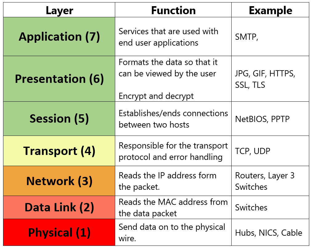
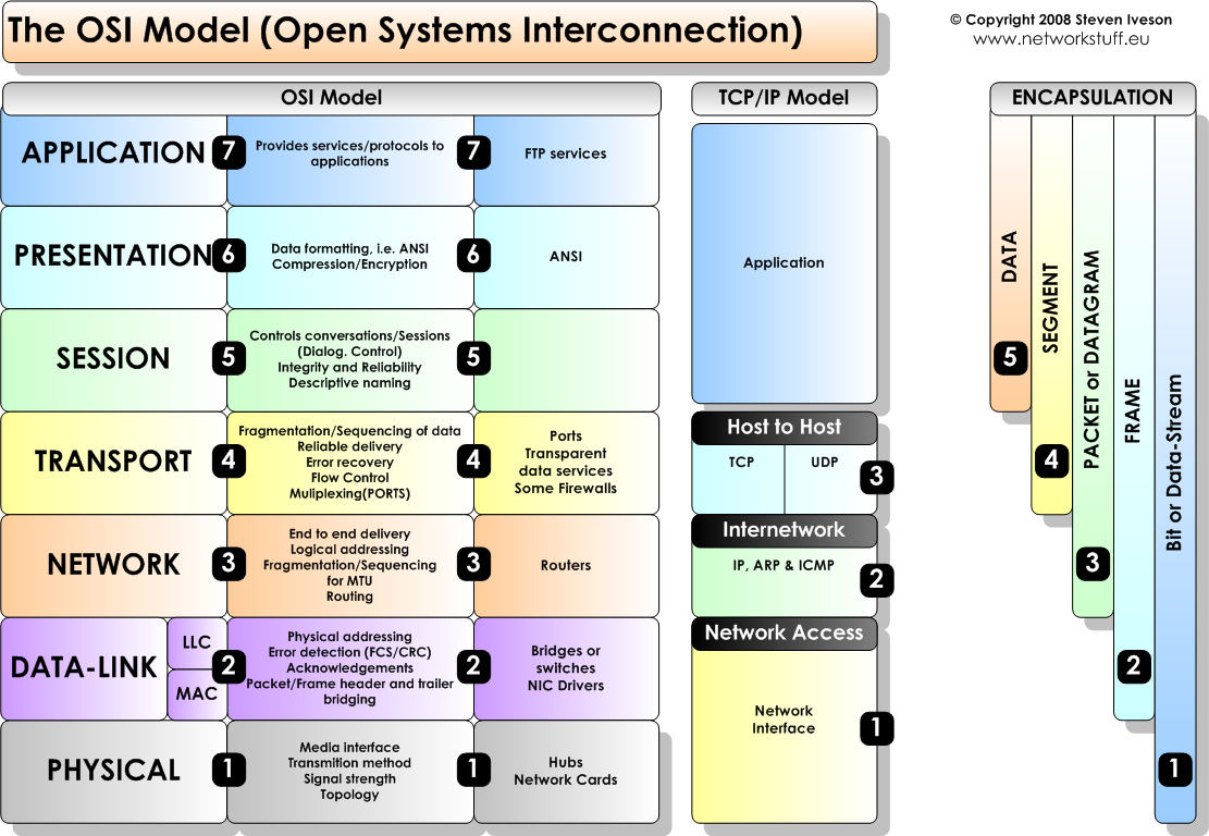
Perhaps OSI 7 layer netwrok protocol model is one of the most widely recognized protocols in the world, it is designed to separate different functionalities based on a hierarchy structure, which is definitely similar to UCIe.
- Hughes T W, Williamson I A D, Minkov M, et al. Wave physics as an analog recurrent neural network[J]. Science advances, 2019, 5(12): eaay6946. 📁[↩]
- Udayanga, Nilan, Arjuna Madanayake, S. I. Hariharan, Jifu Liang, Soumyajit Mandal, Leonid Belostotski, and Len T. Bruton. “A radio frequency analog computer for computational electromagnetics.” IEEE Journal of Solid-State Circuits 56, no. 2 (2020): 440-454.[↩]
- Sharma, Debendra Das, Gerald Pasdast, Zhiguo Qian, and Kemal Aygun. “Universal chiplet interconnect express (UCIe): An open industry standard for innovations with chiplets at package level.” IEEE Transactions on Components, Packaging and Manufacturing Technology 12, no. 9 (2022): 1423-1431.[↩]
- Zhang, S., Z. Li, H. Zhou, R. Li, S. Wang, K. W. Paik, and P. He. “Challenges and recent prospectives of 3D heterogeneous integration.” E-Prime-Advances in Electrical Engineering, Electronics and Energy 2 (2022): 100052. 📁[↩]
- Beyene, Wendemagegnehu T. “Chiplet Technology and Heterogeneous Integration.” 📁[↩]
- Ramamurthy, Anu. “Chiplet Technology & Heterogeneous Integration”, Microchip, (2021). 📁[↩]
- Universial Chiplet Interconnect Express Offical Website[↩]
- Sharma, Debendra D. “Universal chiplet interconnect express (UCIe): Building an open chiplet ecosystem.” UCIE whitepaper (2022).[↩][↩][↩][↩][↩][↩][↩][↩][↩][↩]
- UCIeTM 1.1 Specification: Backward Compatible Evolution of UCIe for Driving an Open Chiplet Ecosystem with New Usage Models[↩][↩][↩][↩][↩][↩][↩]
- Sharma, Debendra Das, et al. “Universal chiplet interconnect express (UCIe): An open industry standard for innovations with chiplets at package level.” IEEE Transactions on Components, Packaging and Manufacturing Technology 12.9 (2022): 1423-1431. 📁[↩][↩]
- UCIe Webinar recordings[↩]
- UCIe Consortium[↩]
- UCIe™ Specifications[↩]
- PCI-SIG: Peripheral Component Interconnect Special Interest Group[↩]
- Compute Express Link™ (CXL™) is an industry-supported Cache-Coherent Interconnect for Processors, Memory Expansion and Accelerators. [↩]
- CXL Consortium[↩]
- e.g., AXI, CHI, SMP coherency protocols, SFI, and CPI[↩][↩]
- Open Domain Specific Architecture(ODSA)[↩]
- Unraveling PCIe 6.0 FLIT Mode Challenges[↩]
- Link State Management[↩]
- Parameter Negotiation[↩]
- for every protocol, UCIe defines 1 mandatory flit mode and optional ones[↩]
- ASE, System in Package (SiP)[↩]
- Transfer per second is also known as sample rate, i.e. the number of data samples captured per second, each sample normally occurring at the clock edge.[↩]
- UCIe Consortium, UCIe™ Packaging Technologies Webinar📺[↩]
- UCIe Consortium, UCIe™ Packaging Technologies Webinar📺[↩]
- Universal Chiplet Interconnect Express (UCIe)®: An open standard for developing a successful chiplet ecosystem. 📁[↩]
- Lau, John H. Heterogeneous integrations. Springer Singapore, 2019.[↩]
- Lau, John H. Chiplet design and heterogeneous integration packaging. Springer Nature, 2023.[↩]
- UCIe Consortium, UCIe™ Packaging Technologies Webinar📺[↩]
- UCIe Consortium, UCIe™ Packaging Technologies Webinar📺[↩]
- UCIe Consortium, UCIe™ Packaging Technologies Webinar📺[↩]
- Compute Express Link™: The Breakthrough CPU-to-Device Interconnect
CXL™[↩] - What is Fan-Out Packaging?[↩]
- Keysight, RF Module Fan-Out Wafer Level (FOWL) Packaging[↩]
- Flip-chip on FO-WLP: assembly process flow.[↩]
- Sundaram, V. and Tummala, R.R. (2014). Interposer Technology. In Handbook of 3D Integration (eds P. Garrou, M. Koyanagi and P. Ramm).[↩][↩]
- High Bandwidth Memory Schematic[↩]
- 国金证券, “先进封装价值量提升叠加需求回暖,封测产业链机遇将至”[↩][↩][↩][↩]
- Through-silicon via[↩]
- Advanced Packaging Part 2 – Review Of Options/Use From Intel, TSMC, Samsung, AMD, ASE, Sony, Micron, SKHynix, YMTC, Tesla, and Nvidia[↩]
- Embedded Multi-Die Interconnect Bridge[↩]
- Mahajan, Ravi, Robert Sankman, Neha Patel, Dae-Woo Kim, Kemal Aygun, Zhiguo Qian, Yidnekachew Mekonnen et al. “Embedded multi-die interconnect bridge (EMIB)–a high density, high bandwidth packaging interconnect.” In 2016 IEEE 66th Electronic Components and Technology Conference (ECTC), pp. 557-565. IEEE, 2016. 📁[↩][↩]
- Back end of line[↩]
- Elsherbini, A. A., S. M. Liff, and J. M. Swan. “Heterogeneous integration using omni-directional interconnect packaging.” In 2019 IEEE International Electron Devices Meeting (IEDM), pp. 19-4. IEEE, 2019. 📁[↩][↩]
- Greek: Unique and Special[↩]
- Intel Foveros Technology Explained[↩]
- UCIe Consortium, UCIe™ Packaging Technologies Webinar📺[↩][↩]
- Foveros Illustration[↩]
- Foveros with EMIB Illustration[↩]
- Foveros Direct: Advanced Packaging Technology to Continue Moore’s Law[↩]
- Omni-Directional Interconnect[↩]
- Chip-on-Wafer-on-Substrate[↩]
- TSMC CoWoS Illustration[↩]
- Douglas Yu, TSMC Packaging Technologies for
Chiplets and 3D[↩][↩] - NEC SX-Aurora Cross Section Illustration[↩]
- high-K MiM Illustration[↩]
- iCAP Illustration[↩]
- Samuel K. Moore, AMD’s Next GPU Is a 3D-Integrated Superchip, IEEE Spectrum[↩][↩]
- AMD EPYC MI300[↩][↩]
- CoWoS®-R[↩]
- CoWoS-R Illustration[↩]
- TSMC OIP: 3DFabric Alliance and 3Dblox[↩]
- CoWoS®-L[↩]
- CoWoS-L Illustration[↩]
- Local Silicon Interconnect[↩][↩][↩]
- Integrated Fan-Out[↩]
- Chiang, Y. P., S. P. Tai, W. C. Wu, John Yeh, C. T. Wang, and C. H. Douglas. “InFO_oS (integrated fan-out on substrate) technology for advanced chiplet integration.” In 2021 IEEE 71st Electronic Components and Technology Conference (ECTC), pp. 130-135. IEEE, 2021. 📁[↩]
- InFO_PoP Illustration[↩]
- Fan-Out Wafer Level Packaging[↩]
- Package on Package[↩]
- Through InFO Via[↩]
- Advanced Packaging 1-2 #TSMC[↩]
- InFO_PoP vs CoWoS with SoC and SoIC[↩]
- System of Integrated Chips[↩]
- Advanced Packaging 1-2 #TSMC📺[↩]
- Chip on Wafer[↩]
- Wafer on Wafer[↩]
- TSMC Announces Wafer-on-Wafer 3D Stacking Technology[↩]
- CoW and WoW comparison[↩]
- Interposer Cube[↩]
- UCIe Consortium, UCIe™ Packaging Technologies Webinar📺[↩]
- Hybrid Substrate Cube[↩]
- eXtended Cube[↩]
- Tom’s Hardware, SK Hynix and Nvidia reportedly working on a radical GPU redesign that 3D-stacks HBM memory directly on top of the processing cores[↩]
- YANGTZE Memory[↩]
- Semicon Talk, Intel Foveros📺[↩]
- ASE, 2.5D and 3D IC Packaging[↩]
- Minkenberg, Cyriel, Rajesh Krishnaswamy, Aaron Zilkie, et al. “Co‐packaged Datacenter Optics: Opportunities and Challenges.” IET Optoelectronics 15, no. 2 (2021): 77-91. 📁[↩]
- data path transfer define arbitrarily[↩]
- Cadence, UCIe PHY and Controller—To Die For[↩]
- version of stacks for D2D adepter to work with[↩]
- Introduction to UCIe Tutorial: UCIe Protocols📺[↩]
- Krishnan, Gokul, Sumit K. Mandal, Manvitha Pannala, Chaitali Chakrabarti, Jae-Sun Seo, Umit Y. Ogras, and Yu Cao. “SIAM: Chiplet-based scalable in-memory acceleration with mesh for deep neural networks.” ACM Transactions on Embedded Computing Systems (TECS) 20, no. 5s (2021): 1-24. 📁[↩]
- NVIDIA V100 TENSOR CORE GPU[↩]
- NVIDIA T4 Tensor Core GPU for AI Inference[↩]
- Mikhaylov, A N, E G Gryaznov, M N Koryazhkina, et al. 2023. “Neuromorphic Computing Based on CMOS-Integrated Memristive Arrays: Current State and Perspectives.” Supercomputing Frontiers and Innovations 10, no. 2: 77–103. 📁[↩]
- Sharma, Harsh, Sumit K. Mandal, Janardhan Rao Doppa, Umit Y. Ogras, and Partha Pratim Pande. “SWAP: A Server-Scale Communication-Aware Chiplet-Based Manycore PIM Accelerator.” IEEE Transactions on Computer-Aided Design of Integrated Circuits and Systems 41, no. 11 (2022): 4145-4156. 📁[↩]
- Goksoy, Ahmet Alper. “In-Memory Computing based Acceleration: Large-Scale to Edge Computing.” PhD diss., Arizona State University, 2023. 📁[↩]
- Lan, Jingjing, Vishnu P. Nambiar, Rheeshaalaen Sabapathy, Mihai Dragos Rotaru, and Anh Tuan Do. “Chiplet-based Architecture Design for Multi-Core Neuromorphic Processor.” In 2021 IEEE 23rd Electronics Packaging Technology Conference (EPTC), pp. 410-412. IEEE, 2021. 📁[↩]
- Nambiar, Vishnu P., Junran Pu, Yun Kwan Lee, Aarthy Mani, T. Luo, L. Yang, Eng-Kiat Koh et al. “0.5 V 4.8 pJ/SOP 0.93\(\mu\mathrm {W}\) Leakage/core Neuromorphic Processor with Asynchronous NoC and Reconfigurable LIF Neuron.” In 2020 IEEE Asian Solid-State Circuits Conference (A-SSCC), pp. 1-4. IEEE, 2020. 📁[↩]
- Vetter, Jeffrey S., Date, Prasanna, Fahim, Farah, Kulkarni, Shruti R., Maksymovych, Petro, Talin, A. Alec, Tallada, Marc Gonzalez, Vanna-iampikul, Pruek, Young, Aaron R., Brooks, David, Cao, Yu, Gu-Yeon, Wei, Lim, Sung Kyu, Liu, Frank, Marinella, Matthew, Sumpter, Bobby, and Miniskar, Narasinga Rao. 2023. “Abisko: Deep codesign of an architecture for spiking neural networks using novel neuromorphic materials”. United States. https://doi.org/10.1177/10943420231178537.[↩]
Leave a Reply