Part of the Train a Transformer on Silicon series — start at #0.
The first version is done: a single GPT-style decoder layer that trains itself on-chip — forward, backprop, and the weight update — taken all the way from a numpy model to a clean 45 nm layout. Here’s what it is, how I checked it, the bug that fooled me, and the numbers.
TL;DR: it trains — bit-exact against the golden model, loss falling 1.21 → 0.17 over 120 steps. All the compute fits in 0.117 mm² of logic; one SRAM macro takes 85% of the 6.99 mm² die. And the single biggest logic block isn’t the matrix engine — it’s LayerNorm backward, at 4× the GEMM’s area.
What v0 is
The plan from #1 was to build the smallest thing that actually trains: a single transformer layer that runs a forward pass, backpropagates, and updates its own weights — in hardware, in fixed point, no GPU in the loop. v0 is that thing.
I wanted it to be a faithful nanoGPT-style decoder layer, not a simplified cartoon of one. So it has all the real pieces:
- LayerNorm with learnable γ and β (and their gradients),
- 1-head causal self-attention — each position attends only to itself and earlier positions,
- a GELU feed-forward network,
- residual connections around both sub-blocks.
It trains with plain SGD on all 10 parameter tensors, against an MSE loss on a causal copy-shift task (no vocabulary yet — that comes in #4). Everything runs in Q16.16 fixed point. The dimensions are small on purpose: embedding width D = 64, feed-forward width DFF = 256, sequence length T = 16, one attention head.
The title of this post is the thing I expected going in. My earlier baseline was an encoder trainer, and the folklore is right: a decoder is an encoder plus a causal mask on the attention. That was almost the whole story. The one genuinely new piece of hardware was LayerNorm, forward and backward — the encoder baseline had used RMSNorm, which is cheaper, but strict nanoGPT fidelity means LayerNorm. That single choice looked harmless at the RTL stage. It came back to bite in the area numbers, and it’s the most interesting result in this post.
The delta from that baseline, in one table:
| encoder baseline | v0 decoder | |
|---|---|---|
| attention | bidirectional | causal (masked) |
| normalization | RMSNorm | LayerNorm — learnable γ/β, and their gradients |
| width | D = 8 | D = 64, DFF = 256 |
| cycles per training step | ~37 k | ~12.76 M |
| hardware added | — | LayerNorm fwd + bwd, causal softmax fwd + bwd |
| hardware reused unchanged | — | GEMM engine (3 modes), GELU + LUTs, elementwise unit |
The mechanism: one datapath, fifty ops
There is no conventional ALU here, and no per-operation hardware. The whole design is one shared sequential datapath that a small controller time-multiplexes across every step of training.
The units on that datapath are:
- a GEMM engine with three modes — A\cdot B (forward), A^{\mathsf{T}}B (weight gradients), and AB^{\mathsf{T}} (input gradients). Those three cover every matrix multiply in both directions.
- LayerNorm forward and LayerNorm backward units,
- causal softmax forward and backward,
- a GELU unit backed by a lookup table,
- an elementwise unit doing ADD / SUB / MUL / SCALE / AXPY — the last of which is the SGD weight update itself.
All of these read and write one single-port RAM. A 50-op microsequencer drives the whole thing: ops 0–14 are the forward pass, ops 15–39 are the backward pass, and ops 40–49 are the SGD updates. It’s the shared-datapath approach I described in #1 — not the fastest way to build this, but small, and it scales by spending more cycles and memory rather than more logic.
The cost of that serialization is time. One full training step is about 12.76 million cycles, which at 100 MHz is roughly 128 ms per step. (For contrast, the old D=8 encoder baseline was 37 k cycles per step — the jump is almost entirely the D=64 GEMMs. Scaling grows cycles and memory, not logic — a theme this series keeps coming back to.)
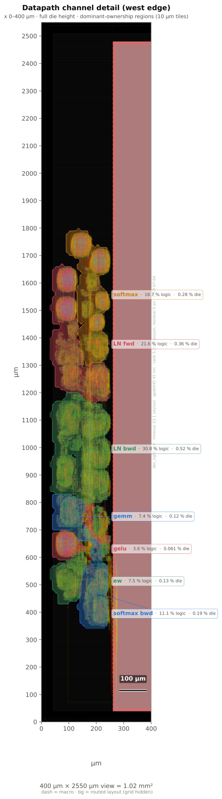
The datapath, not as a cartoon but as placed silicon: the west-edge channel of the routed die, with each unit’s dominant-ownership region outlined. The pink expanse on the right is the SRAM macro they all share.
How I checked it: golden model first
The rule for the whole project (from #1) is check the math before touching the hardware. In practice that was three layers:
- A numpy golden model that implements the entire forward + backward + SGD at the exact Q16.16 precision the hardware uses. The transcendental functions — rsqrt, exp, reciprocal, GELU — aren’t re-derived in numpy; the golden model parses the very same lookup tables out of the RTL source. So the model is bit-identical to the hardware, right down to a quirk where the exp LUT returns
exp(0) = 0.9845instead of exactly 1. Both sides reproduce it deliberately. Bit-exactness depends on sharing the quirks, not fixing them. - That golden backprop is checked against PyTorch autograd. Worst gradient mismatch across all tensors: 2.95 \times 10^{-17} — machine precision. If the math were wrong, this is where I stop, before any RTL exists.
- Then the RTL has to reproduce the golden vectors to the last bit.
And it does. On a single training step, all 10 gradients and all 10 updated weights match the golden model at 0 LSB — exact. Run it for 120 steps and the loss trajectory is identical to golden, step for step, starting 1.2095 → 1.1566 → 1.1087 → …. The training works: MSE falls 1.21 → 0.17, a 7.1× reduction, over 120 SGD steps.
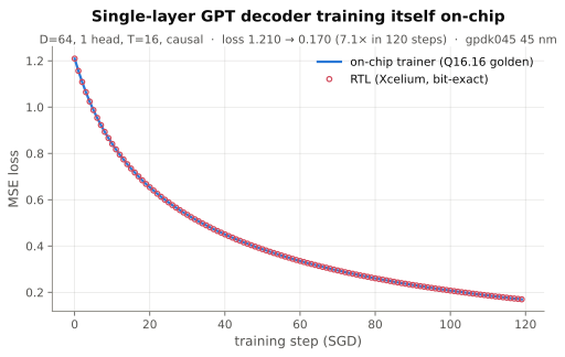
Every red circle is an RTL simulation step; the blue line is the golden model. They are not close — they are bit-identical.
The war story: when the harness lies
This is the part worth reading.
The 1-step result above was bit-exact — every gradient, every updated weight, 0 LSB. So I was confident. Then I ran a multi-step training loop and watched the loss diverge from golden after the very first step. It looked exactly like an RTL bug: some state that’s fine for one step but wrong when you feed the output back in.
I spent a while treating it as one. The thing that cracked it was dumping the forward intermediates and asking a narrower question: if I take the step-1 updated weights and clean-load them into a fresh run, does the forward pass reproduce the golden loss? It did — perfectly. So the weights coming out of step 1 were correct, and the forward pass on correct weights was correct. The RTL was innocent.
The bug was in the testbench. The routine that loaded the training target into memory reused a stale scratch buffer — it $readmemh‘d the target into one array but the load-region logic read a different array. The net effect: the trainer was diligently training against the input instead of the shifted target. Perfectly correct hardware, learning the wrong task.
The lesson generalizes, and it’s now written at the top of my debugging checklist: when 1-step is bit-exact but the N-step trajectory drifts, suspect the harness’s data plumbing before you suspect the DUT. A single step exercises the math; only a multi-step loop exercises the data feedback, and the feedback path runs through the testbench, not the design.
Physical results: synthesis and P&R
With the RTL trusted, I pushed it through synthesis (Cadence Genus) and place-and-route (Cadence Innovus) on a generic educational 45 nm PDK. The data RAM is a blackboxed SRAM macro, counted separately from logic.
Synthesis (100 MHz, 10 ns target):
| metric | value |
|---|---|
| logic cell area | 0.117 mm² |
| cell count | 54,031 |
| timing | met (0 ps slack) |
| power (vectorless, 20% activity) | 1.40 mW |
The power breaks down as 2.5 µW leakage, 0.998 mW internal, 0.400 mW switching. The critical path runs through the LayerNorm backward unit.
Which brings up the surprise. Here is the logic area by block:
| block | area (µm²) |
|---|---|
| layernorm_bwd | 36,164 |
| layernorm_unit | 25,382 |
| softmax_causal | 19,556 |
| softmax_bwd_causal | 13,048 |
| ew_unit | 8,780 |
| gemm_engine | 8,716 |
| gelu_map | 4,268 |
The single biggest logic block is LayerNorm backward — bigger than the matrix-multiply engine itself, by a factor of four. This is the LayerNorm choice from the top of the post coming home. RMSNorm normalizes by a root-mean-square and its backward is comparatively simple; LayerNorm subtracts the mean and divides by the standard deviation, so its backward has a mean/variance coupling term, plus it carries gradients for the learnable γ and β. All of that is real hardware, and it dominates. That’s the concrete price of “strict nanoGPT.”
P&R. The first floorplan was loose: 2860 × 2860 µm = 8.18 mm², with the logic scattered across the die and stranded far from the SRAM macro’s pins. Long nets from the logic out to the macro pins ate into timing. Repacking the logic into a 230 µm channel pressed against the macro’s pin-edge did two things at once — it cut the die by 15% and raised setup slack from +1.76 ns to +2.68 ns, because those long macro-pin nets went away.
| metric | value |
|---|---|
| die | 2740 × 2550 µm = 6.99 mm² |
| SRAM macro | 2440 × 2440 µm = 5.95 mm² (~85% of die) |
| setup slack | +2.680 ns |
| hold slack | +0.062 ns |
| DRC | 0 violations (independently verified) |
The setup headroom is real — this could clock a good deal higher than 100 MHz. On the DRC: I don’t trust the in-flow log’s violation count. The “0” here is from reloading the final database in a fresh tool session and running check_drc, which reported Verification Complete : 0 Viols, 0 Wrngs. Never trust the flow log; reload and re-check.
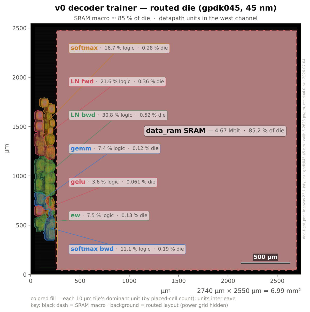
The routed die. Black dash outlines the SRAM macro (4.67 Mbit, 85.2% of the die); every labeled region on the west edge is one datapath unit’s dominant-ownership footprint. The entire GEMM engine is 0.12% of the die.
The memory is the whole story
Look again at that die: ~85% of it is the SRAM macro. The logic is about 1.4%. A chip that trains a transformer, and it’s essentially a block of memory with a rounding error of compute bolted onto the side.
That’s not an accident — it’s the memory map, and the memory map is deliberately naive. Every intermediate value the forward pass produces is kept alive in its own buffer so the backward pass can read it. There are 56 buffers, totaling 145,952 words × 32 bits ≈ 4.67 Mbit. Nothing is ever reused; nothing is freed. It’s the simplest correct thing, and it works, and it’s enormous.
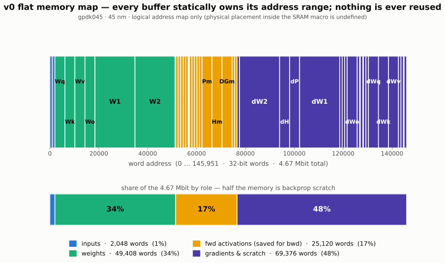
The flat map, drawn to scale. Nearly half the memory is backprop scratch — and most of those buffers are dead for most of a training step.
Which is the real punchline of v0. Building the datapath — the GEMM engine, the norm, the softmax, backprop through all of it — was the part I worried about, and it came out to 0.117 mm² of logic that met timing on the first serious try. The compute was the easy part. The memory is now the job. Most of those 56 buffers are dead for most of a training step; a liveness analysis should let dead buffers be reclaimed and the map packed down hard. That’s the next post.
Honest caveats
Same rules as always for this series:
- It’s a tiny model — D=64, one layer, one head, T=16. This is a demonstration of the mechanism, not a competitive accelerator.
- Generic, educational 45 nm PDK. Representative numbers, not signoff-grade, not a foundry process.
- Power is a vectorless estimate at default activity — not annotated from a real switching trace.
- The power number is logic-only. The SRAM macro is a blackbox to the tools, so its power is not in the 1.40 mW — and on a die that is 85% SRAM, the macro would dominate the real total.
- No tape-out. This is a clean layout in the design tools, not a fabricated chip.
- Top-level IO pins were left unplaced (block-style flow), so connectivity checking flags them as unassigned. That’s cosmetic, and expected.
- The memory map is deliberately unoptimized. The 4.67 Mbit is the flat, every-buffer-alive version. Shrinking it is the point of what comes next.
The full roadmap lives in Part 0 — that’s the hub for the series.
Next up — #3: The Memory Is the Chip. The compute fit in 0.117 mm² and the memory needed 5.95. So before I add a vocabulary or scale anything up, I want to reclaim that memory: liveness analysis on the 56 buffers, free the dead ones, and see how much of that 85% I can give back.
If you build hardware, do ML, or work in EDA — follow along. And if you catch a mistake, tell me. For a series like this, that’s the best thing that can happen.
Leave a Reply