Chip layouts are beautiful, but getting a publication-grade picture of one out of a P&R tool is surprisingly awkward. A GUI screenshot is capped at your monitor’s resolution, carries menu chrome, and is impossible to reproduce exactly a month later. And Cadence Innovus — as of 23.1 — has no vector export of the layout view at all: no PDF, no SVG, no EPS (the entire capture surface is raster).
This post documents the pipeline I ended up with: a scripted, headless flow that produces the figure below — micron axes, a scale bar, per-block annotations whose coordinates come from the P&R database rather than my eyeballs, and embedded metadata so the file explains itself. It runs with one command and produces the same bytes every time.
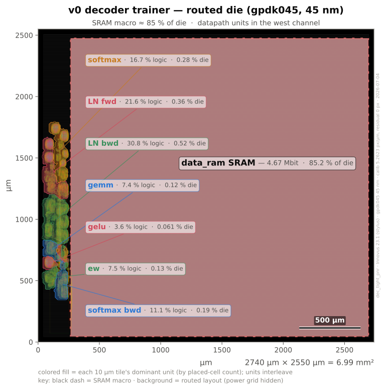
The finished figure (this is the actual SVG). The design is a small on-chip training accelerator on the generic 45 nm educational PDK (gpdk045) — a single SRAM macro takes ~85 % of the die, and all the compute lives in a thin channel on the west edge. You can grab the full-resolution PDF here.
Step 1 — a high-resolution render, with no GUI attached
The one Innovus command that decouples image size from the window is gui_dump_picture, and it goes up to 20,000 × 20,000 pixels:
gui_show
gui_zoom -rect {0 0 2740 2550}            ;# frame exactly the die box (µm)
gui_dump_picture die_16k.png -format PNG -width 16000 -height 14891Two hard-won details:
- Match the pixel aspect ratio to the zoomed box (2740:2550 → 16000:14891). The viewport pads to the window’s aspect otherwise, and you get black letterbox bars baked into the image.
- It needs a GUI window — but not a screen. A virtual framebuffer works:
Xvfb :77 -screen 0 1920x1440x24 -ac &
export DISPLAY=:77
innovus -stylus -files dump.tclDon’t use xvfb-run: its X-authority cookie handshake fails against Innovus, which then falls back to no-window mode silently — every gui_* command becomes a no-op and you get no picture and no error. Raw Xvfb -ac (auth disabled) works.
Before the dump, a handful of legacy display preferences clean the view up enormously — the biggest single win is hiding the power grid, which otherwise buries the standard cells under stripes:
foreach obj {power powerNet mGrid userGrid flightLine} {
    eval_legacy "setLayerPreference $obj -isVisible 0"
}
eval_legacy {redraw}Step 2 — ground truth from the database, not from squinting
Annotating “this region is the softmax unit” by eye is how figures end up subtly wrong. The P&R database knows exactly where everything is, and a batch session (no GUI needed) will tell you:
# macro / die / core boxes
get_db current_design .bbox
get_db inst:u_ram .bbox
# every placed cell of one hierarchical unit
foreach inst [get_db insts -if {.name == uln/*}] {
    set b [get_db $inst .bbox]   ;# accumulate centers to a file
}For this design that yielded the die box, the SRAM macro box, and ~63,000 cell-center coordinates across the seven datapath units.
Step 3 — calibrate pixels to microns from the image itself
The render has unknown margins, so I don’t assume where the die sits in the image. Instead, the wrapper script detects the SRAM macro’s uniform fill rectangle in the PNG (a color threshold plus row/column density bands), and solves the affine pixel↔micron mapping against the macro’s known database box. On this figure the fit reproduces the detected corners with zero-pixel residual at 5.26 px/µm — which is what makes it legitimate to draw micron axes on a raster screenshot.
Step 4 — annotate honestly (bounding boxes lie)
My first version drew each unit’s bounding box. The audit killed that idea: because the placer freely interleaves cells from different units, a unit’s bounding box is mostly empty — the softmax unit’s box contained just 11.8 % softmax silicon, and its box was larger than the LayerNorm-backward unit’s despite having half the logic area. The rectangle wasn’t simplifying; it was misinforming.
The fix: bin the placed-cell field into 10 µm tiles, assign each tile to whichever unit owns the most cells in it, smooth once, and draw each unit as a translucent fill of its owned tiles. Painted area then scales with actual silicon, and each label carries the synthesized numbers directly — e.g. LN bwd · 30.8 % logic · 0.52 % die.
Everything else on the figure is standard matplotlib once the calibration exists: µm axes, a 500 µm scale bar, the area equation pinned to the x-label line, and a muted provenance stamp (database name, tool version, calibration numbers, date) along the right edge.
Step 5 — make the file explain itself
Figures escape their captions — they get downloaded, re-shared, and found months later in a folder. Two cheap defenses:
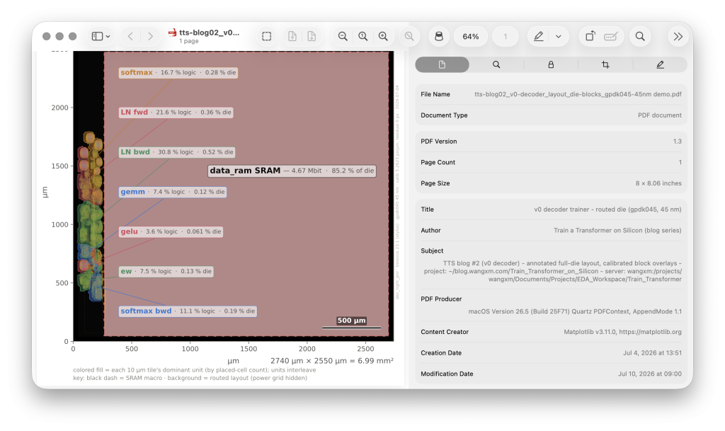
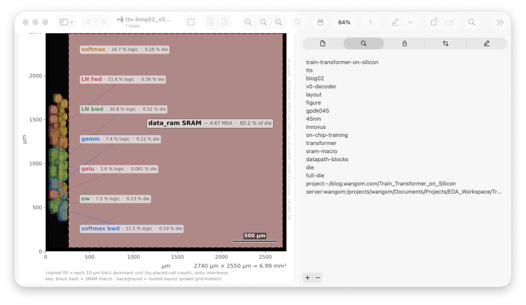
Tags in the filename (<post>_<content>.<ext>), and metadata inside the PDF — matplotlib passes it straight through:
fig.savefig(fname, metadata={
    "Title":    "v0 decoder trainer - routed die (gpdk045, 45 nm)",
    "Subject":  "annotated full-die layout, calibrated block overlays - project: ...",
    "Keywords": "layout, figure, gpdk045, 45nm, innovus, sram-macro, ...",
})macOS Preview shows both panes in its inspector, and Spotlight indexes them — the file becomes findable by any tag it carries:
A note on getting SVG for the web
Since the tool only emits raster, the vector frame (axes, labels, annotations) comes from matplotlib. For the web version you might reach for a PDF→SVG converter — don’t. In my tests both common routes damaged the figure: one flattened every translucent region to opaque (alpha lost), the other dropped all the text. The reliable path is to have matplotlib emit SVG natively alongside the PDF (fig.savefig("fig.svg")), with the embedded raster capped around 4,000 px so the file stays browser-friendly. The figure at the top of this post is exactly that SVG.
Takeaways
gui_dump_picture -width -height(≤ 20,000 px) is the only resolution-controlled export in Innovus; aspect-match it to your zoom box.- Headless works via raw
Xvfb -ac;xvfb-runfails silently. - Hide the power grid before capturing; it’s the single biggest legibility win.
- Pull annotation coordinates from the database, and calibrate the image against a known feature — then your axes mean something.
- Bounding boxes of interleaved placements misinform; per-tile dominant-ownership regions scale with real silicon.
- Name and tag the artifact so it survives being separated from its caption.
The design shown is a small educational project on Cadence’s generic 45 nm PDK (gpdk045) — representative numbers, not signoff-grade, and no tape-out. The pipeline, though, applies to any block you can open in the tool.
Leave a Reply